
New publication in Nature Communications: One light pulse escapes from the other while changing its color
Scientists from Hamburg University of Technology (TUHH), ITMO-University St. Petersburg, Menoufia Univer-sity, University of York, University of St. Andrews, Tyndall-Institute Cork, Sun Yat-sen University Guangzhou, and Helmholtz-Zentrum Geesthacht realized a novel effect in silicon based optical waveguide chips which were particularly designed and fabricated for this nanophotonic experiment. In a special dispersion engineered photonic crystal waveguide a pump light pulse of duration of only six tril-lionths of a second chases a second slower signal light pulse. When the pump pulse reaches the signal pulse, upon interaction, the signal pulse accelerates, changes its frequency, respectively its color, and finally escapes from the pump pulse in forward direction.
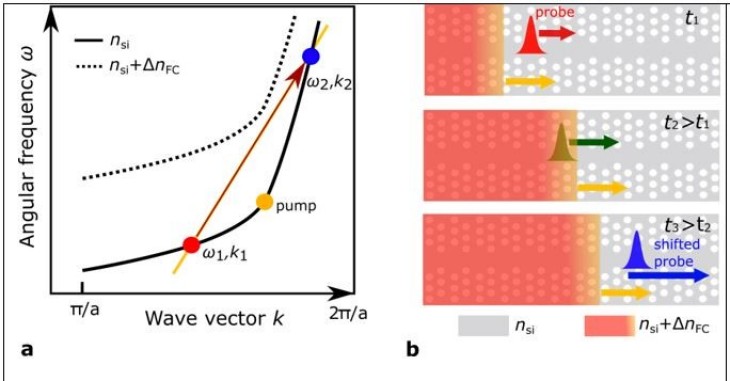
Figure 1: Left (a): Schematic representation of the indirect photonic transition using a band diagram. Solid line: dispersion function of the un-switched photonic crystal waveguide ahead of the moving front. Dashed line: dispersion function of the switched photonic crystal waveguide behind the moving front. Right (b): Schematics of the photonic crystal waveguide (silicon: grey. holes: white). The probing signal with lower frequency (red) stays in the un-switched waveguide, changes its color and accelerates in forward direction (blue). The approaching pump pulse forms a front and the free charge carriers are staying behind the front as a trail (orange). All signals have wavelengths in the vicinity of 1550 nm in the near infrared.
This novel effect is related to the “event horizon” concept which theoretical physicists use to describe the vicini-ty of black holes where this limit marks the “point of no return” of photons. No light particle inside can cross this event horizon to reach the outside world and all these photons are inevitably consumed by the black hole. Such walls for light and changes in the light velocity and color are non-existent in our everyday lives and can be ob-served under very special conditions, only.
How does this work?
The pump pulse generates free electrons in the silicon which creates a fast forward moving front. Since the charge carriers live long compared to the pump pulse duration they are staying behind the propagating front as a trail (Figure 1, right). The conditions have been chosen by careful design of the waveguide such that the signal pulse cannot penetrate into the space behind the front and escapes in forward direction, instead. Since both the frequency and the wave number of the signal are changed, which is quite unusual, the effect is called an “indi-rect” photonic transition (Figure 1, left), which is now theoretically described, numerically modelled and experi-mentally verified.
Under the leadership of the Hamburg based researchers scientific insights of fundamental importance have been gained which, in addition, are crucial for applications in ultra-fast optical telecommunications. As a result of the particular waveguide design, very strong effects can be realized with comparatively small pump power which makes this novel technique particularly attractive for “on-chip” frequency conversion and for all-optical switching.
The work was published on 13.04.2018 in Nature Communications, one of the highest prestigious international scientific journals.
Publication
Reflection from a free carrier front via an intraband indirect photonic transition Mahmoud A. Gaafar, Dirk Jalas, Liam O’Faolain, Juntao Li, Thomas F. Krauss, Alexander Yu. Petrov, and Manfred Eich, Nature Communications 9, 1447 (2018), doi 10.1038/s41467-018-03862-0
Contact
Technische Universität Hamburg-Harburg (TUHH), Institut für Optische und Elektronische Materialien,
Eißendorfer Straße 38, D-21073 Hamburg