
Prof. Dr. Manfred Eich

Prof. Dr. Manfred Eich
Systems Integration
ScientistPhone: +49-(0)-4152-87-2542
Fax: +49-(0)-4152-87-2636
Hydrogen Generation from Photoelectrochemical Water Splitting
Future carbon-free energy systems will rely on the efficient supply with water-originated H2 as a medium for storage and combustion. As a renewable energy alternative to the well-known, yet resource and energy-consuming electrolysis process, photo-electrochemical water splitting where photons from sunlight are used to facilitate or even cause the splitting reaction is considered an attractive option. To realize an efficient photo-electrochemical water splitting process into O2 and H2, many challenges are currently tackled in immense research activities. Enhancing or even driving the water splitting process with the available sunlight energy by using efficient broadband absorber materials as electrodes is one of the currently most promising paths to provide O2 and H2 in different locations, making efforts to separate O2 and H2 unnecessary and operations safer. In our investigations we focus on the fundamental understanding of the optical properties of plasmonic broadband absorbing materials, the injection mechanisms for hot charge carriers generated via this broadband absorption and apply nanostructured metals as combined light absorbers and actively converting electrodes. In detail and in contrast to many other research activities, we focus on the optical metamaterial of “Nanoporous Gold”, a material widely tunable in its macroscopic shape as well as in its microscopic structure. From thin films of some nanometers thickness to macroscopic foils of some micrometers thickness or millimeter-sized cubes or wires etc. many geometries of this material can be realized. Resulting from its spinodal decomposition process of dealloying binary gold-silver alloys, nanoporous gold can be imagined to have a spongy structure with pores and struts, both being variable in size from a few nanometers up to some micrometers. These struts, called ligaments, exhibit a strongly curved surface and are connected with each other in a bicontinuous network which is penetrated by a similar pore network. Although gold is no classical catalyst material due to its weak reactant binding abilities, nanoporous gold was found to show a superior catalytic activity, robustness towards poisoning as well as selectivity towards many currently relevant reactions (such as e.g. methanol oxidation) even beyond those of water splitting. As experiment and simulations reveal, even 100 nm thick layers of this structure enables the nearly 100% efficient broadband optical absorption which is tunable by the porosity, feature size as well as by external parameters, such as an applied potential. Upon this absorption, high energy short lived charge carriers can be generated and extracted into a nearby phase. As we have shown, the efficiency of such a process strongly depends on the metal’s shape, size as well as the place where the excitation occurs. nanoporous gold therein represents an excellent material to study these effects.
Alternatively, an electron deficiency, which is called a “hot hole” can be generated if an electron is lifted from below the Fermi level. We have experimentally shown that both, generated hot electrons as well as hot holes can efficiently be utilized to enhance a chemical reaction close to or directly at the surface of the nanoporous Gold. As the reaction occurs at the surface, it strongly benefits from the high surface-to-volume ratio of nanoporous Gold.
We develop and use (photo-)electrochemical approaches that are capable of quantifying and characterizing such charge carrier transfer processes providing us reliable insights into these not well understood, yet promising phenomena. Being both a size- and property-adjustable metallic nanomaterial as well as a high surface-to-volume ratio and noble electrocatalyst, nanoporous gold represents not just a model material, but also a good basis to investigate fundamental and relevant physico-chemical catalytic processes that will be central in designing ways towards a more efficient and sustainable green energy supply.
-
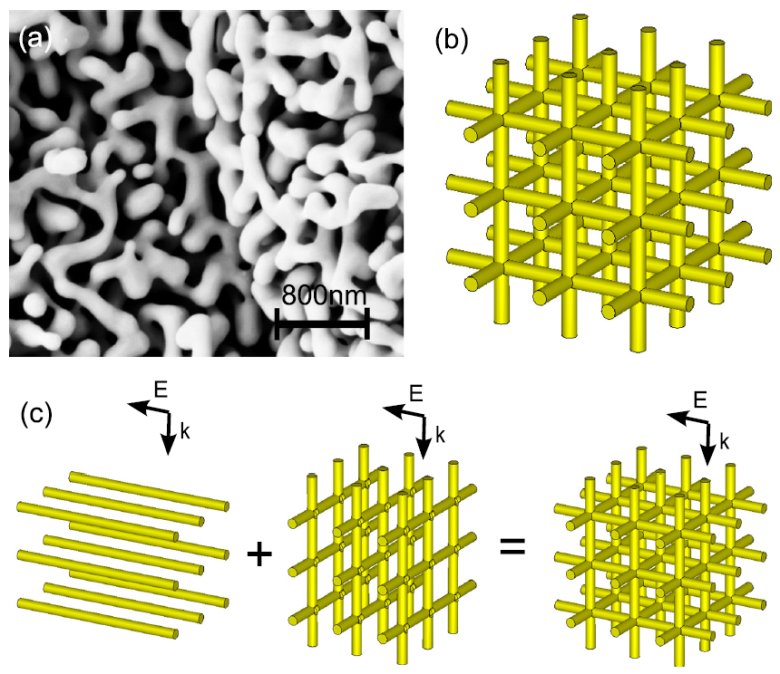 The optical properties of the broadband absorber nanoporous Gold can be modelled effectively using an all-orthogonal wire grid model for effective medium modellation. Under a variation of the volume filling fraction and under the assumption of bulk Au properties, this model predicts important features of the transmission and reflection spectra as a consequence of the addition of a component parallel and a component orthoganoal to the electrical field of the incident optical wave.
 -
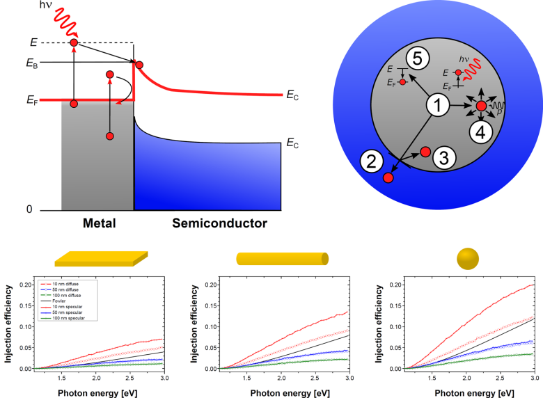 When transferring a hot electron generated in the volume of a metal nanostructure to a nearby phase (e.g. a semiconductor, blue) the electron has to be lifted over a barrier. Depending on the shape (planar, rod or spherical nanoparticle), size and the possible reflection modes of the hot electron at the interface , Monte-Carlo simulation shows that this injection can occur with efficiencies up to 20%.
 -
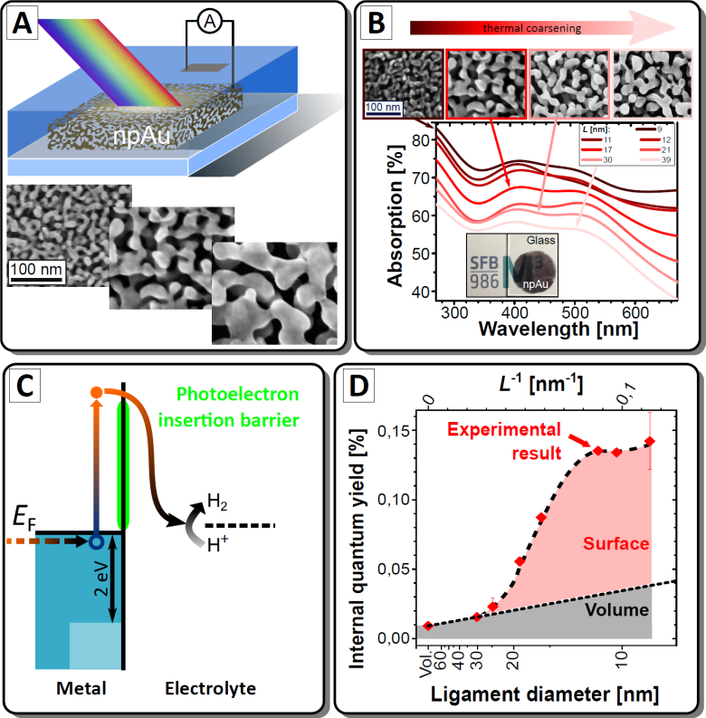 Photon absorption induced hot electron generation in nanoporous gold and their injection into the electrolyte leads leads to hydrogen production in the free electrolyte volume. This process can be followed via an electrical current caused by ilumination. Although the Au structure absorbs broadband (B), the insertion barrier is too high preventing low energy electrons to be inserted (C). The variation of the nanoporous gold’s surface-to-volume ratio enables to differentiate between hot electrons created in the gold volume and those created at the interface, the latter being injected more efficiently. Careful design of the interfacial region can both increase the asborption and the carrier injection efficiency.
Publications - Hydrogen Generation from Photoelectrochemical Water Splitting
- Rodio, M., Graf, M., Schulz, F., Müller, N. S., Eich, M. Lange, H. Experimental Evidence for Non-Thermal Contributions to Plasmon-Enhanced Electrochemical Oxidation Reactions, accepted in ACS Catal. 10, XXX, 2345-2353 2020.
- Hänsch, M., Graf, M., Wang, W., Nefedov, A., Wöll, Chr., Weissmüller, J., Wittstock, G. Compositional Changes at the Ligament Surface in Nanoporous Gold, submitted to ACS Appl. Nano Mater. 2019
- Graf, M.; Jalas, D.; Weissmüller, J.; Petrov, A. Y.; Eich, M. Surface-to-Volume Ratio Drives Photoelelectron Injection from Nanoscale Gold into Electrolyte. ACS Catal. 2019, 9, 3366–3374.
- Haensch, M.; Balboa, L.; Graf, M.; Silva Olaya, A. R.; Weissmüller, J.; Wittstock, G. Mass Transport in Porous Electrodes Studied by Scanning Electrochemical Microscopy – Example of Nanoporous Gold. ChemElectroChem 2019, celc.201900634
- Mahr, C.; Müller-Caspary, K.; Graf, M.; Lackmann, A.; Grieb, T.; Schowalter, M.; Krause, F. F.; Mehrtens, T.; Rosenauer, A. Measurement of Crystal Lattice Strain in Dealloyed Nanoporous Gold. Mater. Res. Lett. 2018, 6 (1), 84–92.
- Blandre, E.; Jalas, D.; Petrov, A. Y.; Eich, M. Limit of Efficiency of Generation of Hot Electrons in Metals and Their Injection inside a Semiconductor Using a Semi-Classical Approach. ACS Photonics 2018, 5, 3613–3620.
Contact details - Hydrogen Generation from Photoelectrochemical Water Splitting
Institute for Materials Technology
Helmholtz Center Geesthacht
Max-Planck-Str. 1
21502 Geesthacht, Germany
And
Institute for Optical and Electronic Materials
Hamburg University of Technology
Eissendorfer Strasse 38
21073 Hamburg, Germany
Photonic Metamaterials for Thermophotovoltaics
Control of thermal radiation at high temperatures is important for waste heat recovery and high-efficiency thermophotovoltaics (TPV) conversion. High temperature stable selective emitters investigated here, which are one-dimensional stacks of alternating metallic and dielectric layers, can significantly increase efficiency and radiative power in thermophotovoltaic (TPV) systems. On the one hand, a high operating temperature is necessary to achieve a large emitted power. According to the Stefan-Boltzmann law, the radiative power of a blackbody is proportional to T^4. On the other hand, spectrally selective emissivity, e.g. the suppression of the emission of low energy (long wavelength) photons, which cannot be converted into electrical power in the photovoltaic cell (PVC) will increase the efficiency. We use a metallic-dielectric optical metamaterial for this purpose which consists of tungsten and hafnia layers and which possesses a hyperbolic dispersion function. The refractory nature of the constituent materials leads to a world class high temperature stability of up to 1400 °C under low oxygen partial pressure conditions. Using state-of-the-art thin-film technology, such spectrally selective emitters are synthesized according to our theory derived designs in order to match the required optical requirements, which mean that they have to be close to black body emission at short wavelengths and exhibit substantially reduced emission at long wavelengths. Above 1400 °C, we observed degradation of the multilayer. The oxidation behavior of tungsten is one crucial point, which depends on the partial pressure of oxygen during application. Thus, proper TPV-designs should aim at either operating at low pressures or under inert gas conditions.
The tailored thin-film properties such as thickness, crystal structure and microstructure are essential for the optical performance in near infrared at high temperatures. Nanometer-sized multilayer structures are fabricated by means of magnetron sputtering under ultra-high vacuum conditions. The advantages of this versatile thin-film method are impressive: materials with high melting point can be deposited, layer thickness can be controlled with high precision up to the picometer-level, sub-atomic sharp interfaces between the adjacent layers, high repeatability and good uniformity can be achieved as well. For the technological transition, lifetime of a metamaterial at a distinct temperature is becoming more and more important. Therefore, high-temperature properties of metamaterials are investigated by X-ray diffraction (ex-situ and in-situ) and high-resolution transmission electron microscopy to carry out the structural changes, phase transformations and chemical reactions. It is worthwhile mentioning that thermal stability of materials relies very heavily not only on their structural but also on their microstructural stability. Consequently, time-dependent thermal processes such as relaxation, recovery, recrystallization and diffusion are in our scientific focus to develop and generate the most promising metamaterial for a long lifetime at highest temperatures in future thermophotovoltaics.
-
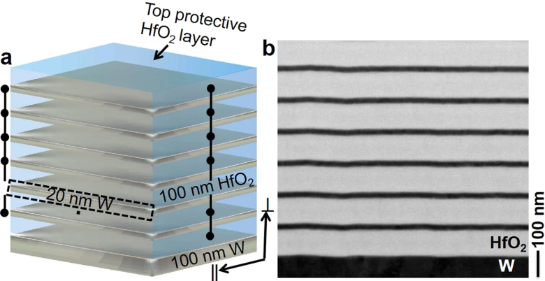 Structure of a 1D layered metamaterial thermal emitter. The metamaterial is constructed of a stack of 6 pairs of 20 nm W and 100 nm HfO2 layers.
 -
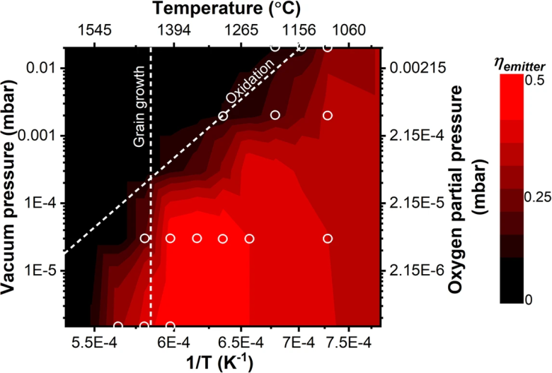 At medium vacuum conditions and temperatures < 1400°C, the metamaterial degrades due to oxidation following an Arrhenius type process. At high vacuum conditions and temperatures > 1400°C, the oxidation is reduced, however, the metamaterial fails due to microstructural changes.
 -
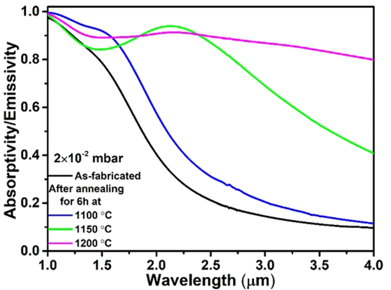 Experimental spectral absorptivity/emissivity of a W/HfO2 metamaterial. Comparison of as prepared and after 6 h annealing at various temperatures and vacuum conditions: In fine-vacuum conditions at 2x10⁻² mbar (a), a significant oxygen partial pressure causes a irreversible change in the spectral selectivity (red shift, blue trace) of the emitter, followed by a complete degradation at 1150°C and 1200°C.
 -
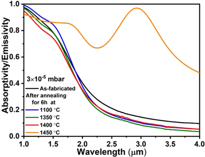 Experimental spectral absorptivity/emissivity of a W/HfO2 metamaterial. Comparison of as prepared and after 6 h annealing at various temperatures and vacuum conditions: At high vacuum conditions at 3x10⁻⁵ mbar (b), the oxidation plays a minor role as degradation mechanism. Microstructural changes of the layers are responsible for the failure at 1450°C.
 -
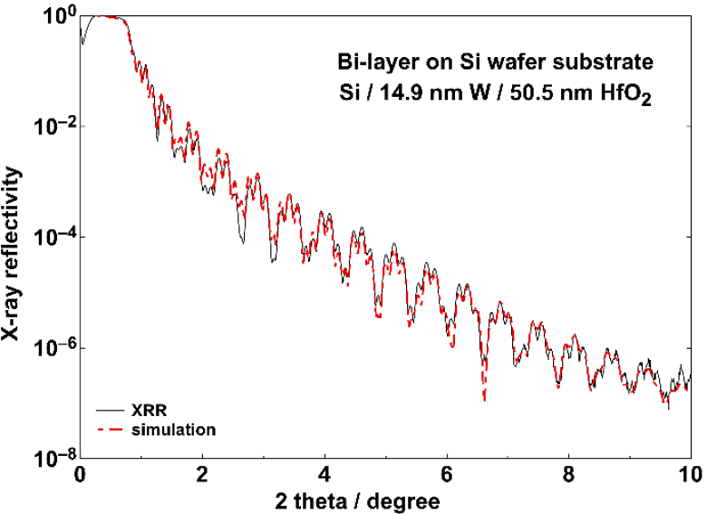 X-ray Characterization of a bi-layer W/HfO2 metamaterial. Layered systems are analyzed by x-ray reflectivity (XRR). Thickness oscillations are used to determine the thickness (vertical spacings of a multilayer stack), the surface and interface roughness and the density of the layers after preparation.
Publications - Photonic Metamaterials for Thermophotovoltaics
- Chirumamilla, M.; Krishnamurthy, G. V.; Knopp, K.; Krekeler, T.; Graf, M.; Jalas, D.; Ritter, M.; Störmer, M.; Petrov, A. Y.; Eich, M. Metamaterial Emitter for Thermophotovoltaics Stable up to 1400 °C. Sci. Rep. 2019, 9 (1), 7241.
- Dyachenko, P.; Molesky, S.; Petrov, A.Yu.; Störmer, M.; Krekeler, T.; Lang, S.; Ritter, M.; Jacob, Z.; Eich, M. Controlling thermal emission with refractory epsilon-near-zero metamaterials via topological transition. Nat. Comms. 2016, 7, 11809.
- Dyachenko, P. N.; do Rosário, J. J.; Leib, E. W.; Petrov, A. Yu.; Störmer, M.; Weller, H.; Vossmeyer, T.; Schneider, G. A.; Eich, M. Refractory absorber/emitter using monolayer of ceramic microparticles. Proc. SPIE 2016, 9885, 98851K.
Contact Details - Photonic Metamaterials for Thermophotovoltaics
Institute for Materials Technology
Helmholtz Center Geesthacht
Max-Planck-Str. 1
21502 Geesthacht, Germany
Institute for Materials Technology
Helmholtz Center Geesthacht
Max-Planck-Str. 1
21502 Geesthacht, Germany
And
Institute for Optical and Electronic Materials
Hamburg University of Technology
Eissendorfer Strasse 38
21073 Hamburg, Germany
Cooperation Partners
- Prof. Dr. Jörg Weißmüller, Institute for Materials Physics and Technology, Hamburg University of Technology, Germany
- Dr. Eric Hill, Institute for Advanced Ceramics, Hamburg University of Technology, Germany
- Dr. Robert Zierold, Department of Physics, University of Hamburg, Germany,
- Prof. Dr. Holger Lange, Department of Chemistry, University of Hamburg
- DFG Sonderforschungsbereich 986 “Tailor-Made Multiscale Material Systems”,
- Prof. Dr. Gunther Wittstock, Department of Chemistry, Carl-von-Ossietzky-Universität Oldenburg, Germany
- Prof. Dr. Marc T. M. Koper, Department of Chemistry, Universiteit Leiden, Netherlands
- Prof. Dr. Forest Chien, Department of Applied Physics, Tunghai University, Taiwan
- Dr. Eva-Maria Steyskal, Institute for Materials Physics, Graz University of Technology, Austria